


3535 Long life Environmental protection energy conservation Large light output angle 2~8 mW
Product Detail
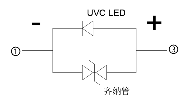
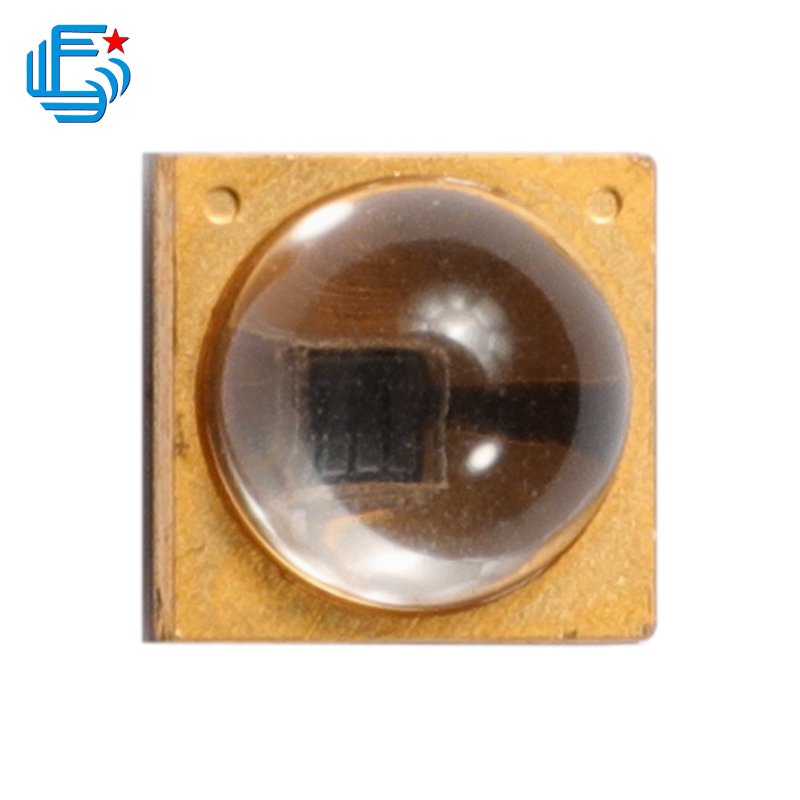
A single device contains two different kinds of chips, UVC and zener diode. Zener diode can protect UVC from ESD
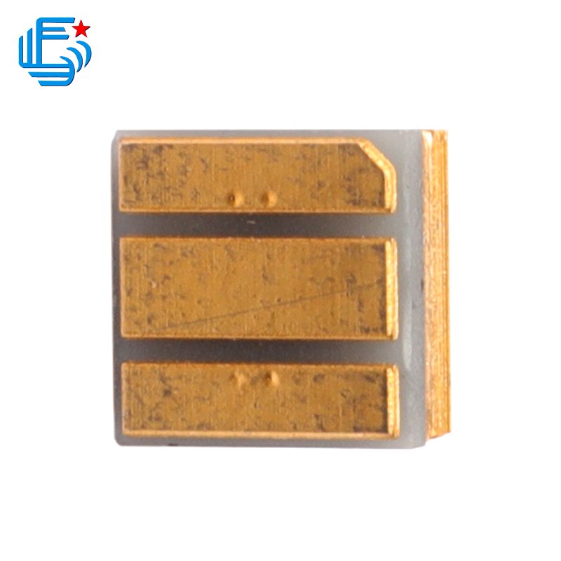
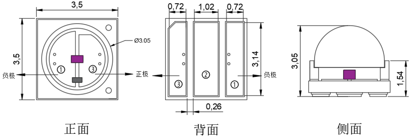
As shown in the figure above, ① is the negative pole and ③ is the positive pole; ② It's a thermal pad
The missing corner on the side and back of the front round hole is the positive mark, and the round hole end of the braided product is the negative mark; There may be no missing corner mark on the back of the real object. Please refer to the drawing and the positive and negative poles of the circuit connection
Due to different batches of stents, there may be slight differences in the physical appearance. Products with different appearances are compatible with each other and do not affect the use
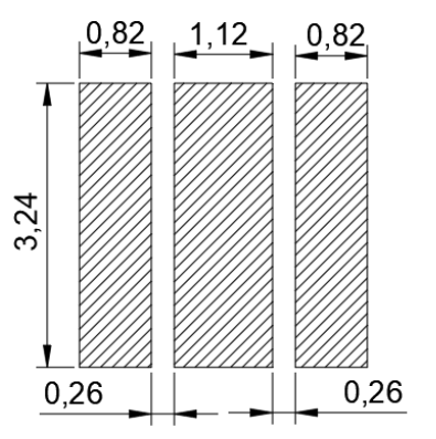
Drawing unit: mm
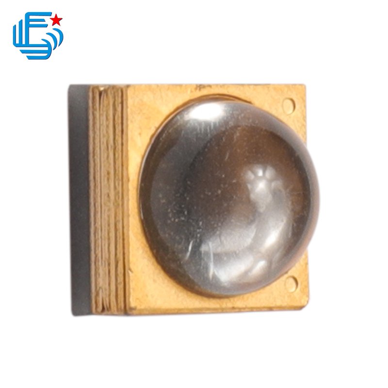
Package: 3535 package, external dimension: 3.5 × three point five × 3.05 (L × W × H) [unit: mm]
Package material: AlN ceramic bracket, hemispherical lens
Number of package chips: 1 pcs
Unless otherwise specified, the dimensional tolerance is ± 0.20 mm
Photoelectric characteristic parameters
UVC photoelectric parameters and spec range (@ 40mA, Ta = 25 ℃, Rh = 30%)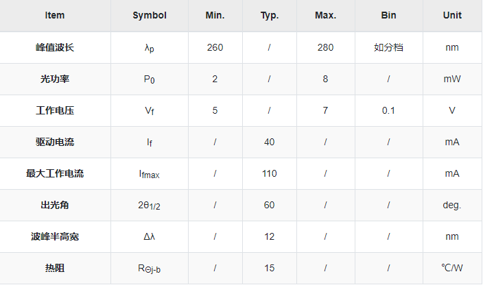
These values are measured by a spectrum analyzer and an integrating sphere measurement system. The tolerances are as follows: working voltage (VF) ± 2%; Optical power (P0): 0 ± 10%; Peak wavelength( λ p): ± 3.0 nm
Although all LEDs are tested by our equipment, some values may be slightly different depending on the conditions of the test equipment.
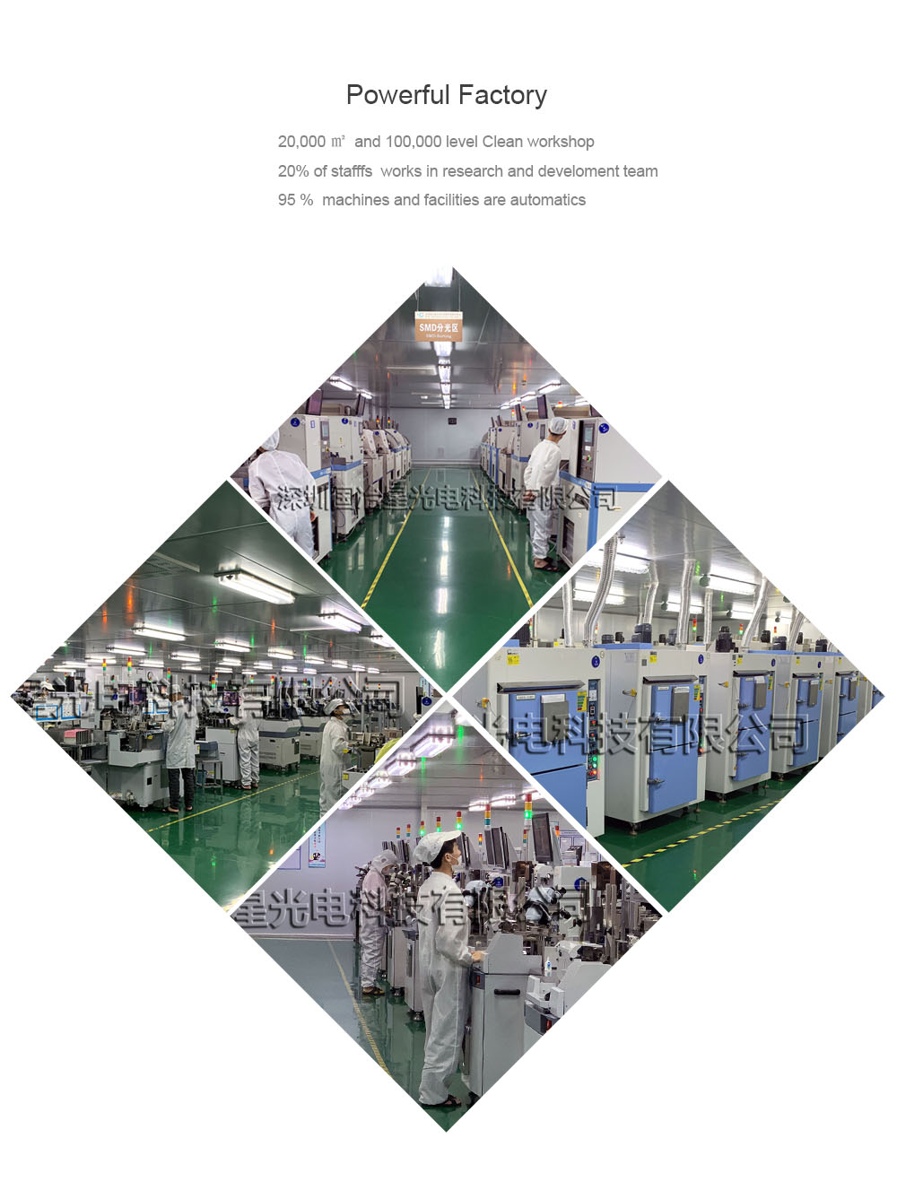
Factory
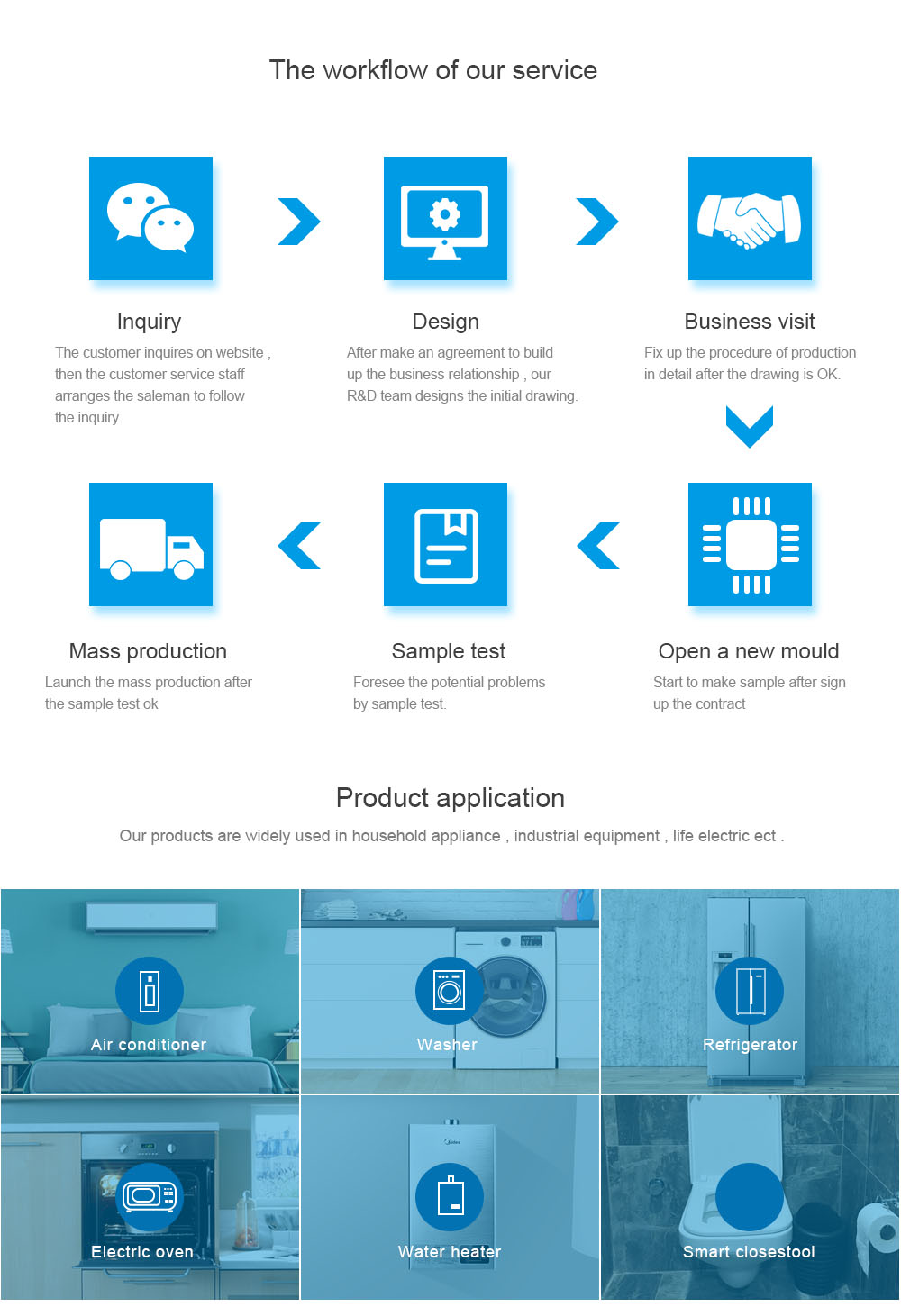
Service


 Copy product links
 Long by picture save/share
INQUIRY


Add Successfully
CONTACT US
 ADD: Building #6, Han’s Laser Industrial Park, No.128 Chongqing Road, Fuyong Town, Bao’an District, Shenzhen, 518103, Guangdong Province, China
 E-Mail:lixt135031@hanslaser.com
Tel/WhatsApp:+86 17724741387


